- 您现在的位置:买卖IC网 > Sheet目录2000 > IDT82V3155PVG (IDT, Integrated Device Technology Inc)IC PLL WAN T1/E1/OC3 DUAL 56SSOP
Functional Description
14
February 20, 2009
IDT82V3155
ENHANCED T1/E1/OC3 WAN PLL WITH DUAL REFERENCE INPUTS
2.7
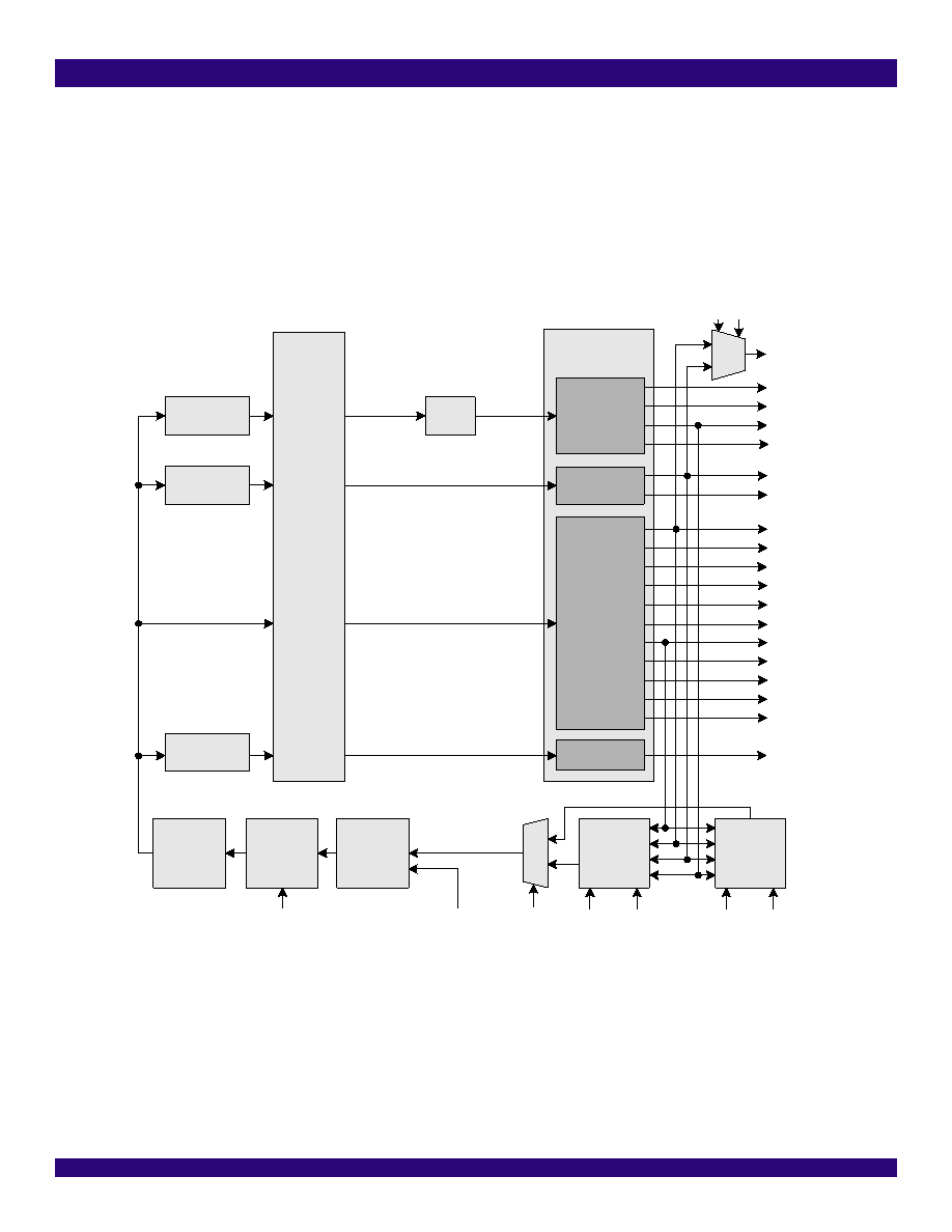
DPLL BLOCK
As shown in Figure - 7, the DPLL Block consists of a Phase Detector,
a Limiter, a Loop Filter, a Digital Control Oscillator and Divider.
2.7.1
PHASE DETECTOR (PHD)
In the Normal mode, the Phase Detector compares the virtual
reference signal from the TIE Control Circuit with the feedback signal
from the Frequency Select Circuit, and outputs an error signal
corresponding to the phase difference. This error signal is sent to the
Limiter circuit for phase slope control.
In the Freerun or Holdover mode, the Frequency Select Circuit, the
Phase Detector and the Limiter are inactive, and the input reference
signal is not used.
2.7.2
LIMITER
The Limiter is used to limit the phase slope. It ensures that the
maximum output phase slope is limited to 5 ns per 125 s for all input
transient conditions. This well meets the AT&T TR62411 and Telcordia
Figure - 7 DPLL Block Diagram
In the Normal mode, the Limiter receives the error signal from the
Phase Detector, limits the phase slope within 5 ns per 125 s and sends
the limited signal to the Loop Filter.
In the Fast Lock mode, the Limiter is disabled, and the DPLL locks to
the input reference within 500 ms, which is much shorter than that in the
Normal mode.
Dig
ital
Con
trol
Osci
llat
or
C32o
C16o
C8o
C4o
C2o
C3o
C6o
F0o
F8o
RSP
TSP
F16o
C1.5o
F32o
Output Interface
T1_Divider
E1_Divider
C6_Divider
Frequency
Selection
Circuit 1
Phase
Detector
Virtual Reference
Fraction_C6
Fraction_T1
24.704 MHz
32.768 MHz
25.248 MHz
Feedback Signal
Limiter
FLOCK
F1_sel1 F1_sel0
C19_Divider
155.52 MHz
F19o
C19o
APLL
19.44 MHz
Fraction_C19
C155NEG
C155POS
IN_sel
F0_sel1 F0_sel0
Frequency
Selection
Circuit 0
C2/C1.5
Loop Filter
Fx_sel1 Fx_sel0 (x = 0 or 1)
发布紧急采购,3分钟左右您将得到回复。
相关PDF资料
IDT82V3202NLG
IC PLL WAN EBU SGL 68-VFQFPN
IDT82V3255TFG
IC PLL WAN SMC STRATUM 3 64-TQFP
IDT82V3280APFG
IC PLL WAN SE STRATUM 2 100TQFP
IDT82V3285AEQG
IC PLL WAN SE STRATUM 100TQFP
IDT82V3285EQG
IC PLL WAN SE STRATUM 100TQFP
IDT82V3288BCG
IC PLL WAN 3E STRATUM 2 208CABGA
IDT82V3355EDG
IC PLL WAN SYNC ETHERNET 64TQFP
IDT82V3358EDG
IC PLL WAN SYNC ETHERNET 64TQFP
相关代理商/技术参数
IDT82V3155PVG8
功能描述:IC PLL WAN T1/E1/OC3 DUAL 56SSOP RoHS:是 类别:集成电路 (IC) >> 时钟/计时 - 专用 系列:- 标准包装:1,500 系列:- 类型:时钟缓冲器/驱动器 PLL:是 主要目的:- 输入:- 输出:- 电路数:- 比率 - 输入:输出:- 差分 - 输入:输出:- 频率 - 最大:- 电源电压:3.3V 工作温度:0°C ~ 70°C 安装类型:表面贴装 封装/外壳:28-SSOP(0.209",5.30mm 宽) 供应商设备封装:28-SSOP 包装:带卷 (TR) 其它名称:93786AFT
IDT82V3202
制造商:IDT 制造商全称:Integrated Device Technology 功能描述:EBU WAN PLL
IDT82V32021
制造商:IDT 制造商全称:Integrated Device Technology 功能描述:EBU WAN PLL
IDT82V32021NLBLANK
制造商:IDT 制造商全称:Integrated Device Technology 功能描述:EBU WAN PLL
IDT82V32021NLGBLANK
制造商:IDT 制造商全称:Integrated Device Technology 功能描述:EBU WAN PLL
IDT82V3202EDGBLANK
制造商:IDT 制造商全称:Integrated Device Technology 功能描述:EBU WAN PLL
IDT82V3202NLBLANK
制造商:IDT 制造商全称:Integrated Device Technology 功能描述:EBU WAN PLL
IDT82V3202NLG
功能描述:IC PLL WAN EBU SGL 68-VFQFPN RoHS:是 类别:集成电路 (IC) >> 时钟/计时 - 专用 系列:- 标准包装:1,500 系列:- 类型:时钟缓冲器/驱动器 PLL:是 主要目的:- 输入:- 输出:- 电路数:- 比率 - 输入:输出:- 差分 - 输入:输出:- 频率 - 最大:- 电源电压:3.3V 工作温度:0°C ~ 70°C 安装类型:表面贴装 封装/外壳:28-SSOP(0.209",5.30mm 宽) 供应商设备封装:28-SSOP 包装:带卷 (TR) 其它名称:93786AFT